DSM/ECU/Reverse Engineering: Difference between revisions
Jump to navigation
Jump to search
Created page with "==Toolbox== * DSLR * Screwdrivers * Tweezers * Solder * Solder Sucker * Solder Wick * Soldering Iron * SMD/Reflow Air Tool * Chamois cloth ===Solvents=== * Acetone * WD-40 *..." |
Tag: Manual revert |
||
| (24 intermediate revisions by the same user not shown) | |||
| Line 1: | Line 1: | ||
=Example= | |||
Here is an example of record keeping of the components and PCB references I did on a 1.8l ECU I reversed as practice: | |||
==Exterior== | |||
<gallery> | |||
Image:MD159561-E2T33674E.png|ECU top | |||
Image:MD159561-E2T33674E-side.png|ECU Exterior, Side | |||
</gallery> | |||
===Top=== | |||
MD159561 | |||
E2T33674E | |||
0607 | |||
Mitsubishi Electric Corp. | |||
Japan | |||
===Side=== | |||
9561 | |||
E2T33674E | |||
Mitsubishi Electric Corp. | |||
Japan | |||
==Interior== | |||
<gallery> | |||
</gallery> | |||
===Processor=== | |||
[[DSM/ECU/TMP76xxx MH6xxx]] | |||
[https://app.gitbook.com/s/-MbMmcGjBEeIX30liMDB/ DSM-ECU Book] | |||
===EPROM=== | |||
* E924 | |||
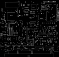
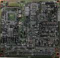
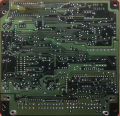
===PCB=== | |||
BOM: [[DSM/ECU/JE331B988B]] | |||
<gallery> | |||
Image:MD159561-E2T33674E-board-overview.png|Board overview | |||
Image:1.8l dsm-ecu-traces.png|Copper traces of PCB | |||
Image:JE331B-silkscreen.png|Silkscreen | |||
Image:JE331B-top.png|Top layer photo | |||
Image:JE331B-bottom.png|Bottom layer photo | |||
</gallery> | |||
==How-To== | |||
===Hardware=== | |||
# Obtain ECU | |||
# Take external photographs | |||
#* Mostly for all the numbers and letters/the stickers | |||
# Open ECU | |||
# Remove PCB | |||
# TAKE MORE PICTURES (before you touch anything else) | |||
#* The code on the plug socket | |||
#* The microprocessor | |||
#* The EPROM (if there is one) | |||
#* Any and all visible marking on components | |||
#* The ENTIRE board on BOTH sides | |||
# RECORD all components with visible markings, decode resistor values | |||
#* This means a table with the PCB Silkscreen references and the components values | |||
# ACETONE bath | |||
#* This is to remove all the conformal coating junk that interferes with reading markings AND the ability to probe, test, and desolder | |||
# SCRUB with Toothbrush, Q-Tips | |||
# PHOTOGRAPH and RECORD any newly visible information | |||
# REMOVE any components with known values: | |||
## Electrolytic capacitors can go first | |||
## Then any ICs | |||
## Resistors with the bands already decoded | |||
## Connectors | |||
# REMOVE components with unknown values ONE AT A TIME | |||
## SMD Capacitors and Transistors are good examples | |||
## Remove one, use the Multimeter and/or LCR meter to get values and RECORD them in the table | |||
# Eventually you will be left with a BARE BOARD | |||
# SPRAY and WIPE DOWN the bare PCB with WD-40 to clean up any remaining conformal coating and junk | |||
#* This preps the board for nice clear photographs | |||
# PHOTOGRAPH both sides of the PCB | |||
#* Get ONE photo of EACH side of the PCB | |||
#* Flat | |||
#* In focus | |||
#* Dead-on photos with no perspective error | |||
#* Use a tripod | |||
#* Use lighting | |||
#* Use a remote shutter-release to eliminate shake from the image | |||
===Digitization=== | |||
# Do color correction in darktable | |||
# Import to GiMP and isolate the Silkscreen to generate a silkscreen layer | |||
# Import into Inkscape to create a vector of the copper traces | |||
# Use the last two steps to import into KiCad | |||
#* Recreate the PCB | |||
#* Create a schematic from the PCB | |||
===Result=== | |||
# A BOM of sorts | |||
#* List of all the components, and their values and locations on the PCB | |||
# A Schematic of the electrical connections | |||
# A PCB layout | |||
# Lots of photos | |||
# ROM dumps of all ROM, Internal ROM and EPROM | |||
# Disassembly of all ROM, Internal and External | |||
==Toolbox== | ==Toolbox== | ||
===Tools=== | |||
* Screwdrivers | * Screwdrivers | ||
* Tweezers | * Tweezers | ||
| Line 9: | Line 115: | ||
* SMD/Reflow Air Tool | * SMD/Reflow Air Tool | ||
* Chamois cloth | * Chamois cloth | ||
* Multimeter | |||
* LCR Meter | |||
===Solvents=== | ===Solvents=== | ||
* Acetone | * Acetone | ||
* 99% Isopropyl alcohol | |||
* WD-40 | * WD-40 | ||
* Flux | * Flux | ||
* Flux cleaner | * Flux cleaner | ||
* | * H2O | ||
== | ===Camera=== | ||
* DSLR | |||
* Tripod | |||
* Circular-polarized lens | |||
* Remote shutter-release | |||
* Lighting | |||
===Software=== | |||
* Darktable | |||
* GiMP | |||
* Inkscape | |||
* KiCad | |||
Latest revision as of 19:05, 23 February 2026
Example
Here is an example of record keeping of the components and PCB references I did on a 1.8l ECU I reversed as practice:
Exterior
-
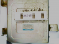 ECU top
 -
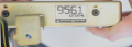 ECU Exterior, Side

Top
 MD159561
 E2T33674E
  0607
 Mitsubishi Electric Corp.
 Japan
Side
 9561
 E2T33674E
 Mitsubishi Electric Corp.
 Japan
Interior
Processor
EPROM
- E924
PCB
BOM: DSM/ECU/JE331B988B
-
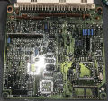 Board overview
 -
 Copper traces of PCB
 -
 Silkscreen
 -
 Top layer photo
 -
 Bottom layer photo


How-To
Hardware
- Obtain ECU
- Take external photographs
- Mostly for all the numbers and letters/the stickers
- Open ECU
- Remove PCB
- TAKE MORE PICTURES (before you touch anything else)
- The code on the plug socket
- The microprocessor
- The EPROM (if there is one)
- Any and all visible marking on components
- The ENTIRE board on BOTH sides
- RECORD all components with visible markings, decode resistor values
- This means a table with the PCB Silkscreen references and the components values
- ACETONE bath
- This is to remove all the conformal coating junk that interferes with reading markings AND the ability to probe, test, and desolder
- SCRUB with Toothbrush, Q-Tips
- PHOTOGRAPH and RECORD any newly visible information
- REMOVE any components with known values:
- Electrolytic capacitors can go first
- Then any ICs
- Resistors with the bands already decoded
- Connectors
- REMOVE components with unknown values ONE AT A TIME
- SMD Capacitors and Transistors are good examples
- Remove one, use the Multimeter and/or LCR meter to get values and RECORD them in the table
- Eventually you will be left with a BARE BOARD
- SPRAY and WIPE DOWN the bare PCB with WD-40 to clean up any remaining conformal coating and junk
- This preps the board for nice clear photographs
- PHOTOGRAPH both sides of the PCB
- Get ONE photo of EACH side of the PCB
- Flat
- In focus
- Dead-on photos with no perspective error
- Use a tripod
- Use lighting
- Use a remote shutter-release to eliminate shake from the image
Digitization
- Do color correction in darktable
- Import to GiMP and isolate the Silkscreen to generate a silkscreen layer
- Import into Inkscape to create a vector of the copper traces
- Use the last two steps to import into KiCad
- Recreate the PCB
- Create a schematic from the PCB
Result
- A BOM of sorts
- List of all the components, and their values and locations on the PCB
- A Schematic of the electrical connections
- A PCB layout
- Lots of photos
- ROM dumps of all ROM, Internal ROM and EPROM
- Disassembly of all ROM, Internal and External
Toolbox
Tools
- Screwdrivers
- Tweezers
- Solder
- Solder Sucker
- Solder Wick
- Soldering Iron
- SMD/Reflow Air Tool
- Chamois cloth
- Multimeter
- LCR Meter
Solvents
- Acetone
- 99% Isopropyl alcohol
- WD-40
- Flux
- Flux cleaner
- H2O
Camera
- DSLR
- Tripod
- Circular-polarized lens
- Remote shutter-release
- Lighting
Software
- Darktable
- GiMP
- Inkscape
- KiCad